SEMICONDUCTOR INDUSTRY

Optical metrology solutions to answer broad optical testing needs in lithography manufacturing

Semiconductor  | Optical metrology solutions for the semiconductor industry | Phasics

Lithography systems for the semiconductor industry rely on extremely complex laser sources and optical systems. The Phasics SID4 range spans from the ultraviolet (UV) to the longwave infrared (LWIR) and has been proven extremely valuable in the semiconductor industry for the qualification of such optical systems at their designed wavelength. Engineers in research and development or manufacturing use the SID4 wavefront sensors for laser sources and optical systems alignment and metrology.

Operators in a semiconductor factory.

UV and DUV laser system testing

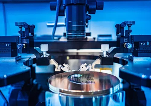
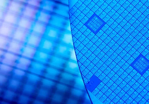
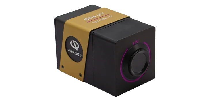
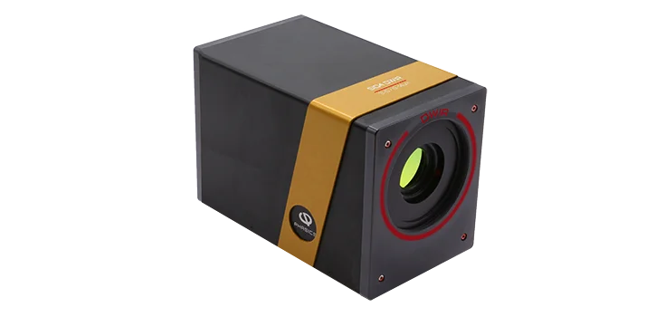
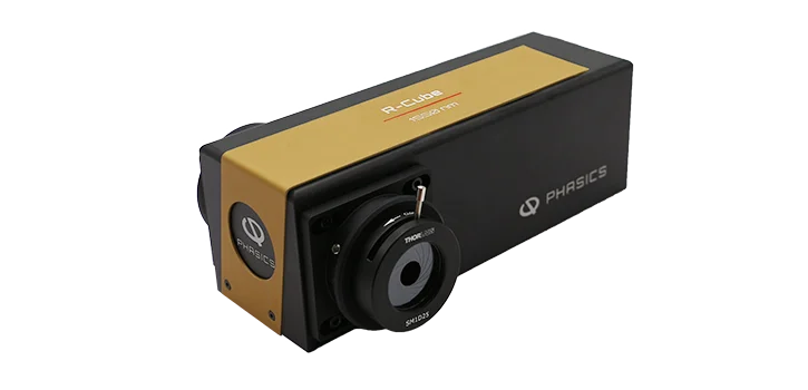
The Phasics SID4 UV wavefront sensors give access to a complete laser characterization in a single measurement. SID4 UV wavefront sensors are the ideal tool to support lithography system manufacturers and integrators to align, qualify, and monitor their ultra-violet sources and systems.

Learn more
Illumination optics and a wafer

Beam correction and control

Control of the laser quality and beam shaping with adaptive optics is applicable to lithography machines. The combination of SID4's unique wavefront sensor, OASys expert adaptive optics software, and dedicated deformable mirrors represent a robust solution for lithography machine manufacturers. 

Learn more
Zoom on a wafer

Wafer inspection

All along the lithography process, inspection of the wafers is performed. Inspection is a key part in the wafer manufacturing process. Coupling high dynamic range, nanometric wavefront sensitivities, and high resolution, Phasics' technology is a great candidate to be integrated in wafer inspection machines. 

Learn more

Related Products

Download


Sign up to receive the latest updates and news